

PCB Design and Development Services in India: From Concept to Manufacturing
Electronic products are becoming an essential part of modern industries. From industrial automation equipment and IoT devices to monitoring systems and embedded electronics, almost every smart product depends on a reliable electronic circuit.
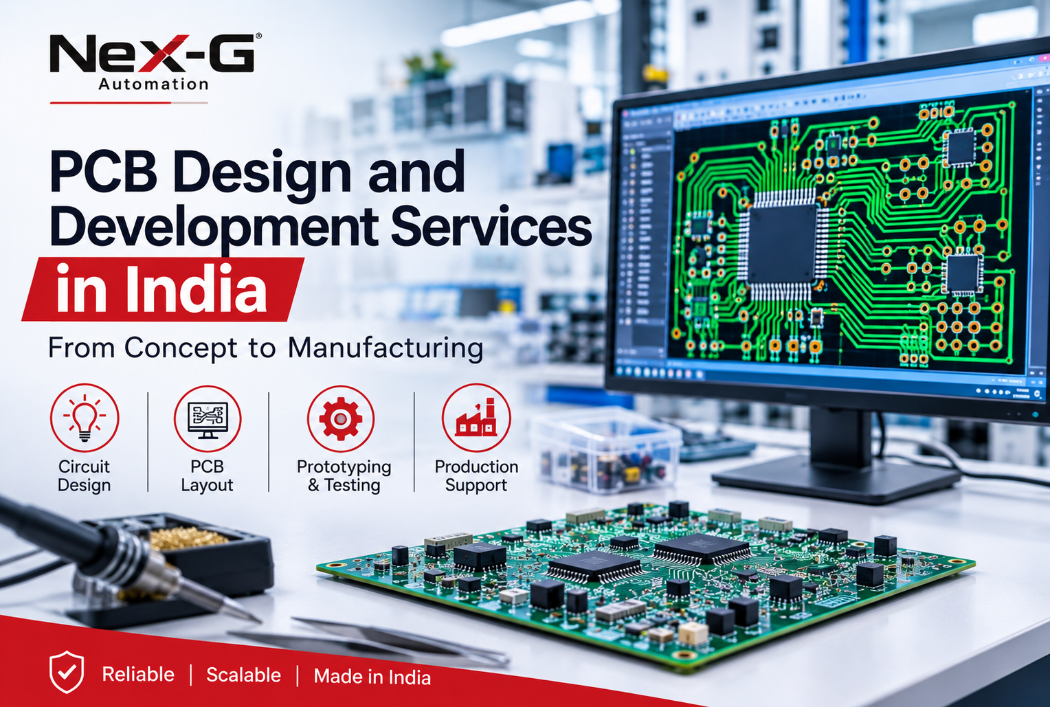
At the centre of these electronic systems is the Printed Circuit Board (PCB). A well-designed PCB provides the electrical connections and physical platform required for electronic components to communicate and operate together.
However, developing a PCB involves more than arranging electronic components on a board. It requires circuit planning, component selection, schematic design, PCB layout, signal considerations, prototyping and testing.
Businesses looking for PCB design services in India need a development approach that considers the complete application, performance requirements and future manufacturing needs.
In this article, we explore the PCB design process, its important stages, applications and factors to consider when choosing a PCB design and development partner.
What Is PCB Design?
Printed Circuit Board (PCB) design is the process of
developing the electrical circuit and physical board layout used in an
electronic device.
A PCB contains conductive copper pathways that connect
electronic components such as resistors, capacitors, integrated circuits,
connectors and microcontrollers.
The PCB provides a structured platform for electronic
components and helps ensure that electrical signals and power are distributed
according to the design requirements.
Depending on the application, PCBs can be designed as
single-layer, double-layer or multilayer boards.
Why Is Professional PCB Design Important?
PCB design directly influences the performance, reliability
and manufacturability of an electronic product. A properly designed PCB helps
address several engineering considerations:
·
Electrical performance: Appropriate circuit
connections and routing help maintain reliable operation.
·
Component placement: Strategic component positioning
supports efficient circuit operation and assembly.
·
Thermal management: PCB layout must consider
heat-producing components and heat dissipation.
·
Signal integrity: Routing, grounding and layout
decisions help manage unwanted interference and signal degradation.
·
Manufacturability: Design decisions should
account for fabrication and assembly capabilities.
·
Product reliability: Design reviews and testing
help identify potential issues before production.
A PCB should therefore be designed according to the intended
operating environment, electrical requirements and manufacturing process.
PCB Design and Development Process
A structured development process helps convert an electronic
concept into a functional PCB.
1. Requirement Analysis and Project Planning
The first stage involves understanding the purpose and
operating requirements of the electronic product. Important information
includes:
·
Intended application and operating environment
·
Required input and output interfaces
·
Power supply requirements
·
Microcontroller or processor requirements
·
Communication protocols
·
Board dimensions and mechanical constraints
·
Expected production quantity
This information establishes the technical direction for the
project.
2. Electronic Circuit and Schematic Design
After requirement analysis, the electronic circuit is
developed. The schematic represents the electrical connections between
components and defines how the circuit is expected to function.
·
Component selection
·
Power supply design
·
Microcontroller interfacing
·
Sensor and actuator connections
·
Communication interfaces
·
Protection circuits
A carefully reviewed schematic helps reduce design errors
before PCB layout begins.
3. PCB Layout Design
PCB layout converts the electrical schematic into a physical
board design. Components are positioned according to functional requirements,
board dimensions and routing constraints.
·
Component placement
·
Copper trace routing
·
Ground and power planes
·
Layer stack-up planning
·
Connector positioning
·
Thermal considerations
·
Design-rule checking
For complex electronics, signal integrity, electromagnetic
compatibility and high-speed routing considerations may also be important.
4. Design Verification and Documentation
Before fabrication, the PCB layout should be reviewed
against the electrical and mechanical requirements. Design verification may
include:
·
Design Rule Check (DRC)
·
Electrical Rule Check (ERC)
·
Component footprint verification
·
Clearance and spacing checks
·
Schematic-to-layout consistency
·
Manufacturing documentation review
The resulting documentation may include Gerber or other
fabrication data, drill files, assembly drawings and a Bill of Materials (BOM),
depending on the manufacturing requirements.
5. PCB Prototyping
Prototyping provides an opportunity to evaluate the physical
board before committing to larger production quantities. A prototype can be
used to assess component placement, electrical functionality, connectivity and
overall product behaviour.
6. Testing and Design Improvements
The prototype is evaluated to identify issues that may
require engineering changes. Depending on the project, testing may include:
·
Power-up and functional testing
·
Input and output verification
·
Communication testing
·
Thermal evaluation
·
Environmental testing
·
Integration with other electronic modules
Identified issues can be addressed through PCB revisions
before production.
7. Manufacturing Preparation
After design validation, the project can move towards
manufacturing. This stage involves preparing the required fabrication and
assembly documentation, confirming component availability and reviewing
production requirements. Design-for-manufacturing and design-for-assembly
considerations help improve production readiness.
Types of PCB Design
Single-Layer PCB
A single-layer PCB contains one conductive copper layer and
is generally suitable for simpler electronic circuits. Typical applications
include basic control circuits and simple electronic devices.
Double-Layer PCB
A double-layer PCB contains conductive copper layers on both
sides of the board. It offers greater routing flexibility and is commonly used
in control boards, embedded systems and industrial electronics.
Multilayer PCB
A multilayer PCB contains three or more conductive layers
separated by insulating materials. It is suitable for more complex electronic
designs that require higher routing density, additional power and ground
planes, or controlled signal routing.
The correct PCB structure depends on the circuit complexity,
electrical requirements, available space and project budget.
Applications of PCB Design in Industrial Automation
Industrial IoT Devices
IoT hardware uses electronic circuits to collect data from
sensors, process information and communicate with monitoring platforms.
Industrial Control Systems
Custom PCB designs can support embedded control electronics,
interface boards and automation-related equipment.
Data Logging and Monitoring Equipment
Electronic boards support sensor interfacing, data
acquisition, processing and communication in monitoring devices.
RFID-Based Systems
RFID-related electronics can be used in identification,
tracking and inventory management applications.
Safety and Alert Devices
Electronic circuits support the operation of industrial
warning systems, monitoring devices and emergency alert equipment.
How to Choose a PCB Design and Development Company in India?
Selecting an appropriate PCB development partner is an
important part of electronics product development. Before choosing a service
provider, consider the following factors:
1.
Technical understanding: The development team
should understand the intended application and electrical requirements.
2.
Circuit design capability: Evaluate experience
in schematic development, component selection and circuit integration.
3.
PCB layout expertise: Check the ability to handle
board complexity, routing and manufacturing constraints.
4.
Prototyping and testing: Understand how
prototypes are evaluated and design changes are managed.
5.
Documentation: Confirm the availability of
relevant design and manufacturing files.
6.
Communication: Clear communication and
engineering coordination are essential throughout the project.
7.
Production readiness: Consider whether the
design approach supports future manufacturing requirements.
The right partner should understand the complete product
requirement rather than treating PCB layout as an isolated activity.
PCB Design and Development at Nex-G Automation
Nex-G Automation LLP works in industrial automation, IoT and
electronic hardware development.
Our engineering-oriented approach focuses on understanding
application requirements and developing suitable electronic solutions for
industrial and automation-related applications.
PCB design and development projects can involve circuit
planning, electronic component integration, PCB layout and prototype development
according to the project scope.
Whether the requirement involves an industrial control
circuit, an IoT-based device or a custom electronic application, the
development process should begin with clearly defined technical requirements.
Businesses looking for electronics development support can
connect with Nex-G Automation to discuss their project requirements.
Frequently Asked Questions
What are PCB design services?
PCB design services involve developing electronic
schematics, selecting components, creating PCB layouts and preparing design
documentation for electronic products.
How long does PCB design and development take?
The development timeline depends on circuit complexity,
component availability, board layers, design requirements and prototype testing.
A simple PCB may require considerably less time than a complex industrial
electronics board.
What is the difference between PCB design and PCB manufacturing?
PCB design involves creating the electrical circuit and
physical board layout. PCB manufacturing involves fabricating the physical
board and, when required, assembling electronic components.
What files are required for PCB manufacturing?
Depending on the manufacturer and process, files may include
Gerber or other fabrication data, drill files, board specifications, assembly
drawings and a Bill of Materials.
Can PCB design support industrial IoT products?
Yes. PCB design is an important part of industrial IoT
hardware, including sensor interfaces, communication modules, embedded
controllers and data acquisition devices.
Why is PCB prototyping important?
Prototyping allows engineers to evaluate the design, test
functionality and identify potential issues before proceeding to larger
production quantities.
Conclusion
PCB design is a foundational stage in developing reliable
electronic products. From circuit planning and component selection to layout,
prototyping and manufacturing preparation, each stage contributes to the final
product's performance and usability.
For businesses developing industrial electronics, automation
equipment or IoT devices, selecting an appropriate PCB design and development
partner can help establish a structured path from concept to production.
Looking for PCB
Design and Development Support in India? Contact Nex-G Automation to
discuss your electronic hardware requirements and explore suitable development
approaches.
Relevant Nex-G page: Nex-G
PCB Design service page
A reliable PCB design process requires attention to design rules, component
selection, manufacturability and assembly quality. Industry organisations such
as IPC provide widely recognised standards
and resources that support quality and consistency in electronics manufacturing.
During the assembly planning stage, engineers can also refer to the IPC
PCB Assembly Checklist to understand important inspection and assembly
considerations.
India's electronics manufacturing ecosystem is also receiving policy support
through initiatives such as the Government of India's Scheme
for Promotion of Manufacturing of Electronic Components and Semiconductors.